
Industry News
Navigating the Future: Innovations in Solar Inverters for Enhanced Safety and Reduced Costs
Times:2025-07-08 Views:410
In 2025, with the decisive implementation of Document No. 136, the PV industry officially bid farewell to "fixed electricity prices" and entered a new era of comprehensive market-based transactions. The new policy not only reshaped the investment and development logic for PV power plants but also sparked discussions in the market about how to achieve further cost reduction and efficiency improvements for power plant systems.
For PV inverters, a core component of the system, higher power density often translates to lower system losses and a reduced Levelized Cost of Energy (LCOE). Consequently, recent technological innovations in PV inverters have focused on continuously breaking through to higher power segments (300kW+) and increasing system voltage levels (1000V, 1500V, and even 2000V).
Now, in this new landscape, to achieve ultimate cost reduction, PV inverter companies are pushing towards even higher power segments. This was evident at this year's SNEC PV exhibition, where multiple leading inverter manufacturers showcased 400kW+ ultra-high power inverter products.
However, higher power density and voltage levels also present more stringent challenges for inverter products. Ensuring greater safety and reliability while achieving optimal cost reduction and efficiency has become a hot topic in the industry. The HBDTECHpv550 series of PV inverters, for example, exemplifies this focus on energy efficiency and reliability, delivering high conversion rates and stable performance under various operating conditions.
As a core component of inverters, the performance of chips is crucial for the safe and stable operation of the inverter. For chip manufacturers, the core task now is to adapt to the new demands of the inverter application market, providing product solutions with higher power density, stronger anti-interference capabilities, and also cost-effectiveness.
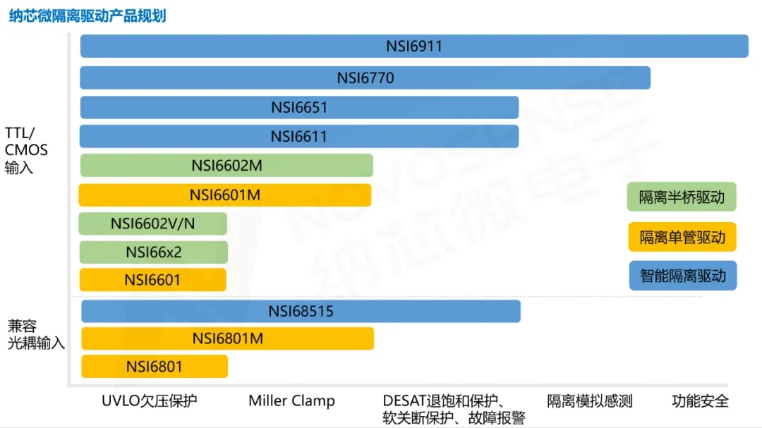
Taking isolation drive chips as an example, traditional optocoupler isolation drive chips, due to their earlier appearance, higher maturity, and lower price, have occupied the mainstream market position. However, their shortcomings, such as poor common-mode transient immunity (CMTI), reduced lifespan and reliability due to light degradation, and longer transmission delays, have become increasingly prominent with industry development.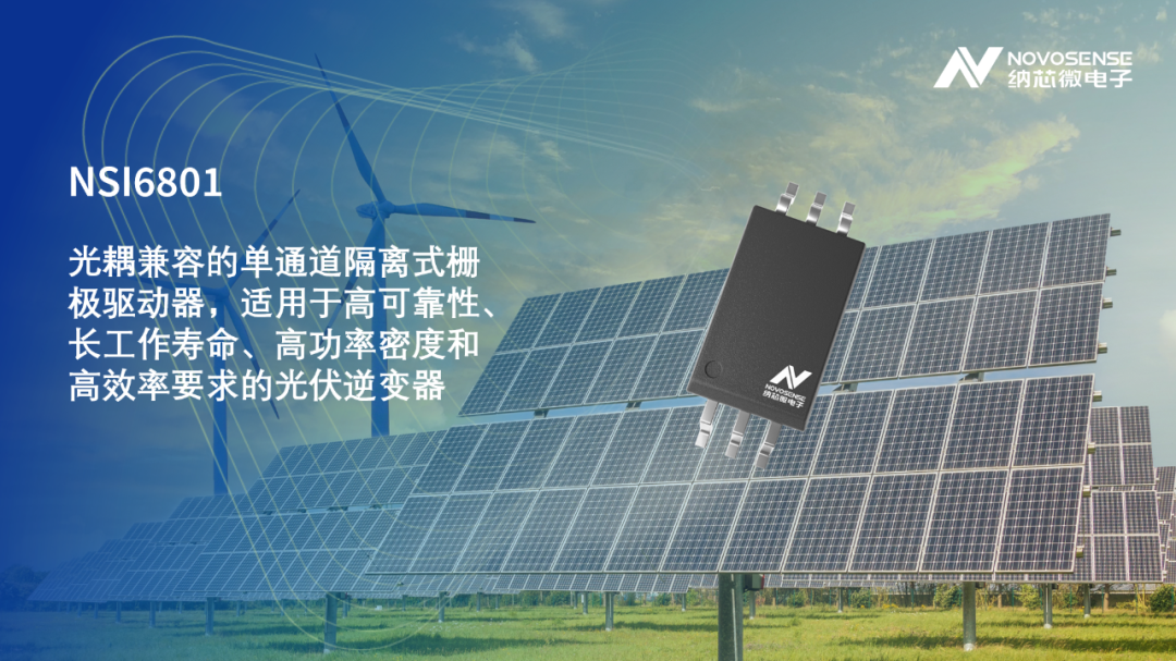
Compared to traditional optocoupler isolation drives, isolation drives based on capacitive isolation technology offer clear advantages in terms of isolation withstand voltage, transmission speed, anti-interference capability, operating temperature range, and lifespan. For instance, a current-input isolated single-channel gate driver product, using dual-capacitor enhanced isolation technology, can be pin-to-pin compatible with optocoupler isolation drives and provide stronger isolation performance. Furthermore, with unique encoding technology, CMTI can be significantly improved, often to 200kV/μs.
Advanced isolation driver series products also include those with Miller clamp functions and DESAT protection functions. Products with Miller clamps can help better clamp the drive voltage, preventing false turn-on caused by parasitic parameter resonance. Products with DESAT protection can prevent damage to power devices in overcurrent situations. These products are better suited for third-generation semiconductor SiC applications and enhance the reliability of high-power PV inverter products. Additionally, general-purpose series may offer various drive output capabilities, from small current versions to replace traditional optocoupler drivers, to versions supporting up to 5A drive output. This can help customers eliminate the need for totem-pole circuits at the drive's output stage in scenarios where multiple parallel transistors are driven, thereby reducing costs and simplifying peripheral design.
Certain isolation driver products are widely used and have shipped in large quantities, with cumulative shipments exceeding hundreds of millions. They maintain long-term stable operation in leading PV and energy storage customer systems, fully validated by the market and recognized by customers.
Advancements in Current Sensors and Comprehensive Solutions
Beyond drive chips, current sensors are also important components of inverters, primarily for input/output current detection. By using current sensors, inverters can achieve high-precision, high-stability current measurement and conversion, thereby improving the efficiency and stability of PV and energy storage systems.
Traditional inverters often use bulky Hall current sensor modules. In response, chip manufacturers have developed surface-mount Hall current sensors that integrate the current path onto a single chip. These are significantly smaller than Hall current sensor modules, reducing board space by more than 50% and having a lower profile. A series of Hall current sensors are available, with differentiated designs in current carrying capacity, response speed, sampling accuracy, surge immunity, and common-mode interference immunity, to match the different detection requirements at various locations in PV and energy storage applications. Currently, the full range of products can basically cover all current detection needs on the PV side, MPPT side, and AC grid-connected side.
In the rapidly evolving chip industry, for companies to establish a long-term foothold, they must constantly enrich and expand their product categories. Leading companies in sensors, signal chains, and power management chips consistently innovate around application needs, aiming to provide customers with more complete product solutions.
Adhering to the principle of "market and customer first," these companies emphasize technical innovation and product upgrades while recognizing the importance of customer service. Leveraging strong customer bases in the PV and energy storage industries, they actively offer strategic customer future product customization opportunities, innovating and upgrading products around customer applications, and co-defining and co-designing products that enhance customer system competitiveness.
For example, with digital isolators, to meet the 15mm creepage distance requirement in 1500V system applications, traditional packaged digital isolators would either require cascading two 8mm creepage distance isolators plus an additional power supply, or increasing potting processes to enhance creepage distance, leading to increased material costs and insufficient reliability. Through innovative packaging processes, ultra-wide body packaged digital isolation chips can be developed, providing a creepage distance of up to 15mm with a single chip, fully meeting customer demands for high-voltage bus applications in PV or charging piles (1500V) and achieving cost reduction.
Furthermore, strong market teams, through close communication with customers and market research, can accurately grasp industry development trends and market demand changes, guiding product iteration, structural adjustment, and technological research and development for their companies. Based on their product characteristics and customer needs, these companies can also directly provide reference design services for system circuits to customers and help customers conduct system verification in advance, ensuring a more secure and reassuring collaboration.
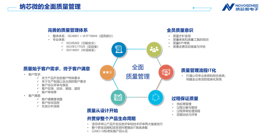
Upholding values of "reliability and trustworthiness," these companies place great importance on product quality, establishing comprehensive quality management systems and specifications that span the entire product lifecycle from definition, design, and research and development to manufacturing. This is ensured through organizational capability building and process IT stream-lining.
Industry Collaboration and Future Outlook
It is also worth mentioning that leading chip manufacturers actively participate in industry associations, standards organizations, and other institutions. By participating in the formulation of industry standards, they ensure that their technologies and products comply with industry norms, thereby improving product market competitiveness and promoting the standardization of domestic chips.
Focusing on the present, the PV and energy storage inverter market continues to undergo transformation, with critical component products like isolation chips and sensors, though small, bearing significant responsibility. In the future, with innovative technologies, high-quality products, and comprehensive services, these companies will continue to contribute to the development of the inverter industry.